So I have been building pedals for a little over a year. In that time I have always hand wired my switches unless the breakout boards were supplied with the circuit.
I felt it was time to take the next step and create my own PCBs. I have breadboarded a few circuits and I want to put a few into production. As a test I created my own breakout board for the 3PDT. I usually see them for $1 a board. So I did a little digging around, found some information on panelizing your layouts using a Sparkfun ULP for panelization and got to work.
Setup
The links above are to an article I found on panelizing. Use that tutorial to setup Eagle so that you can panelize your circuits. You should also go to the JLCPCB article on installing the CAM settings for them in Eagle as well.
The rest of the article is based on thiese already being done.
Create Schematic
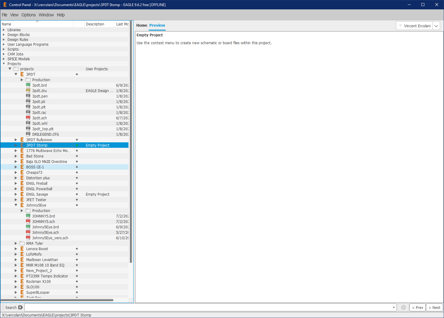
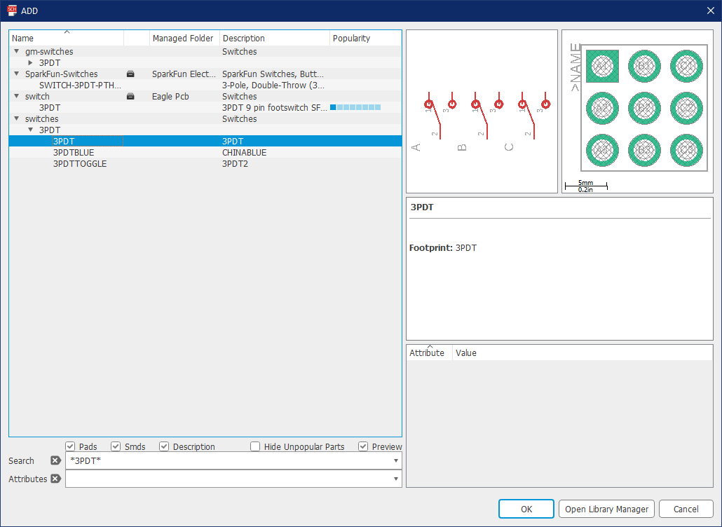
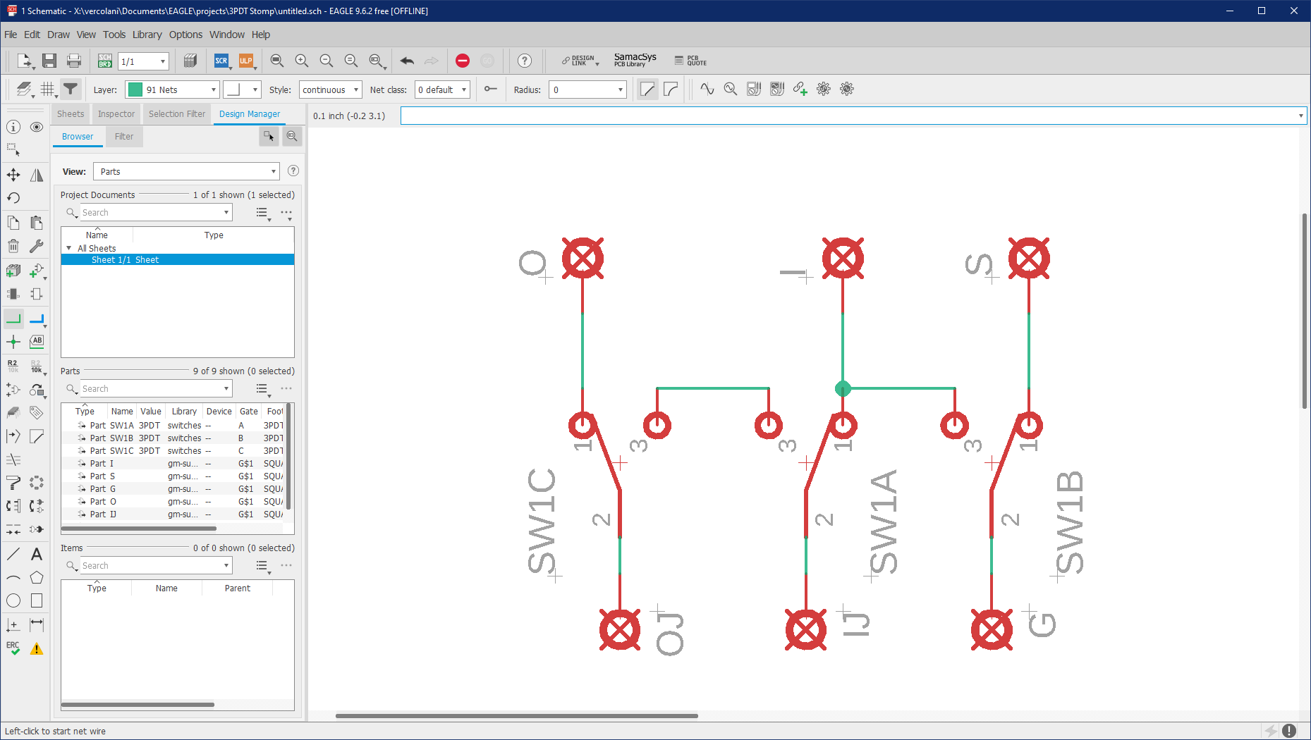
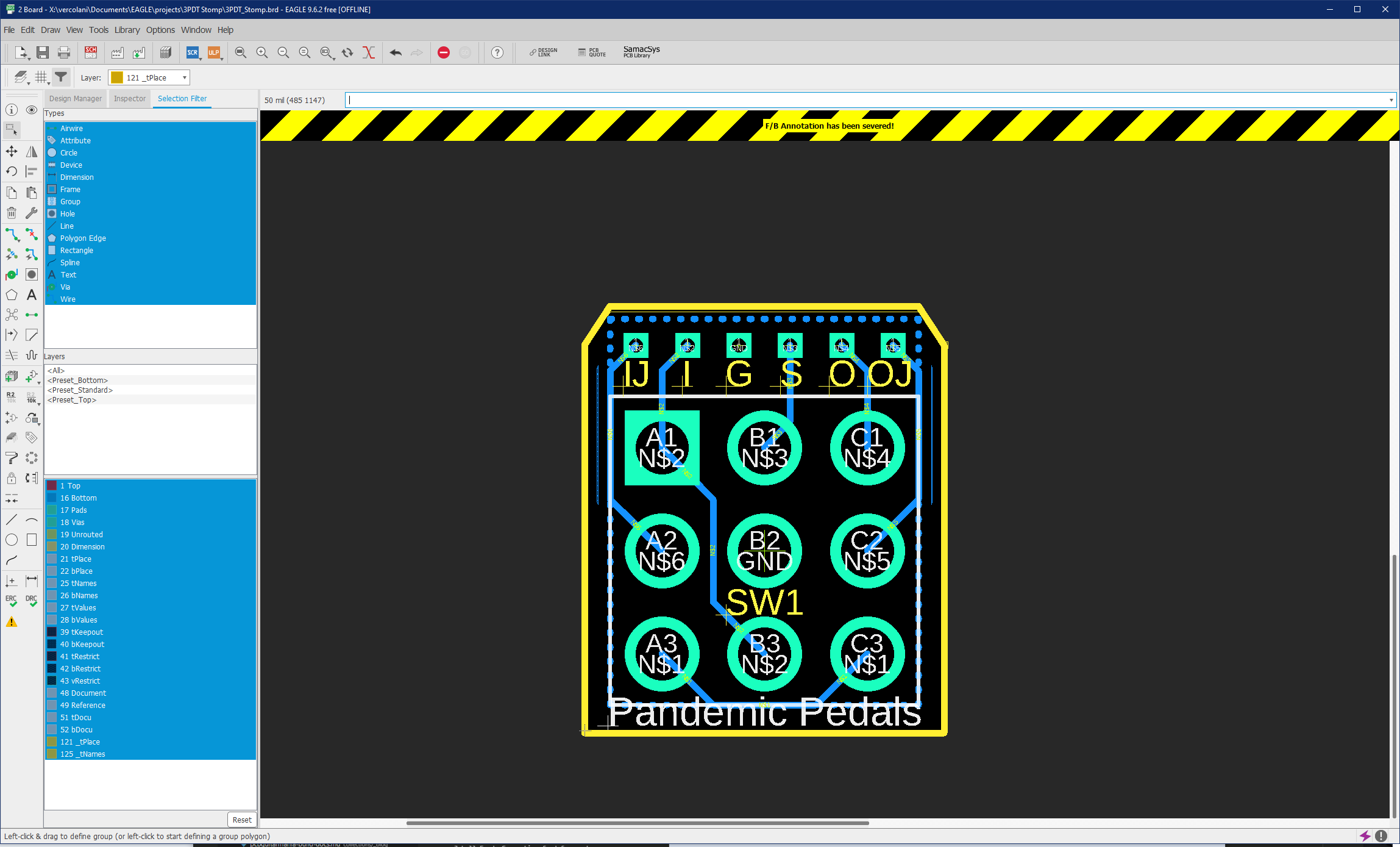
The first thing you want to do is create a project in Eagle and create a schematic. I chose the 3PDT stomp under switches because it has the large circular holes. I also used square pads for all the pads here so that I had more metal surface to solder to. The boards I show later use the round pads.
Create Board
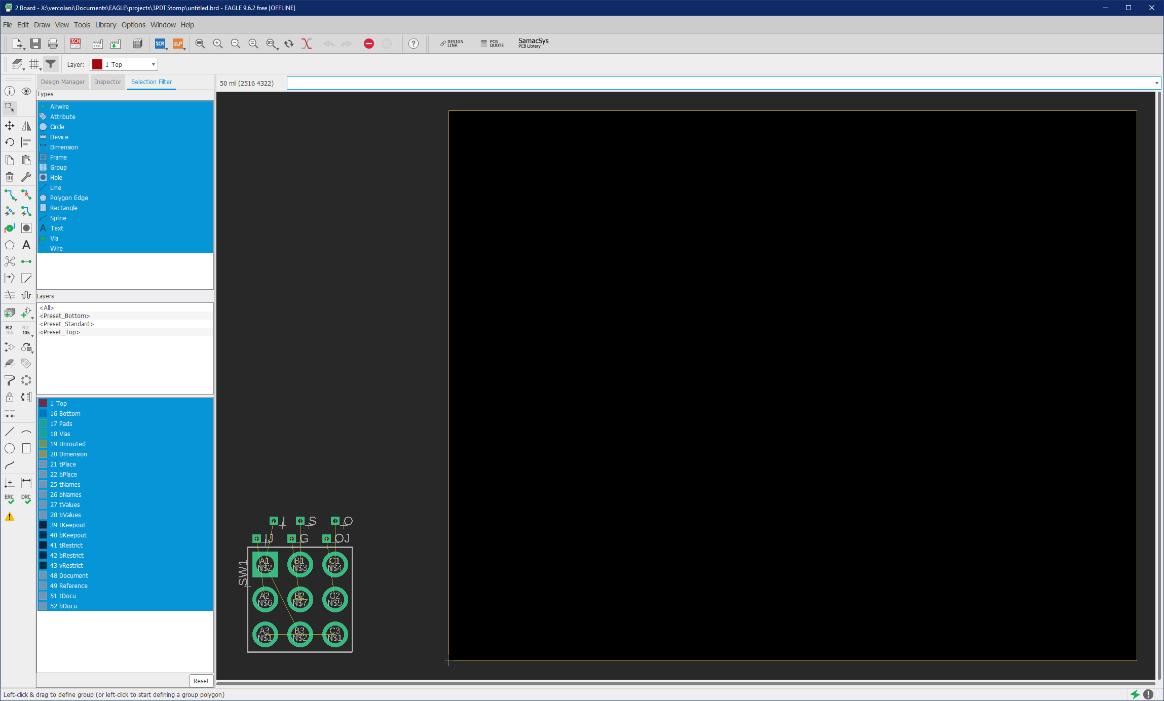
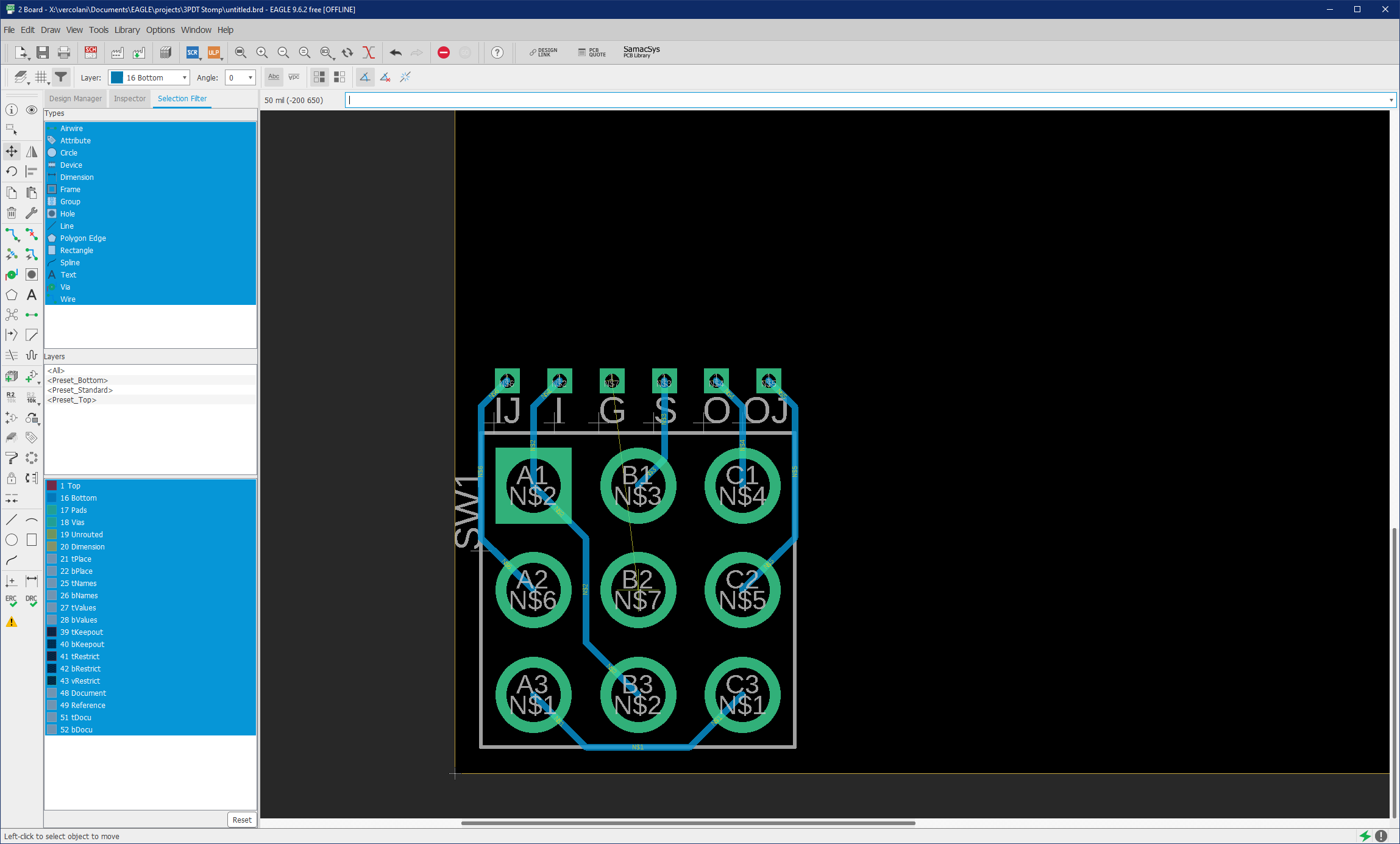
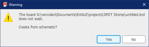
I create my board by first clicking on the green and gray “SCH/BRD” button to auto create the board. I then layout the parts. I use 12mil for my airwires. I also use the pentagon to create my ratsnest. I put all my traces on the bottom of the board. This one can be done on a single layer. Also you can delete the yellow board outline and create your own on the dimension layer.
Panelizing
Once you have the board you would like to panelize you will need to:
- close the schematic
- select the entire board
- copy it
- click on the ULP button
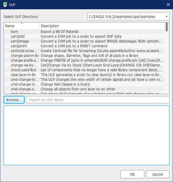
At this point the ULP dialog will pop up. You will need to hit the browse button and choose the Sparkfun Panelizer ULP that you installed earlier. This will allow all your panels to have the same label names for components. It also tiles your layout on the panel.
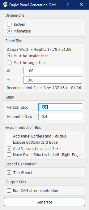
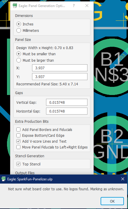
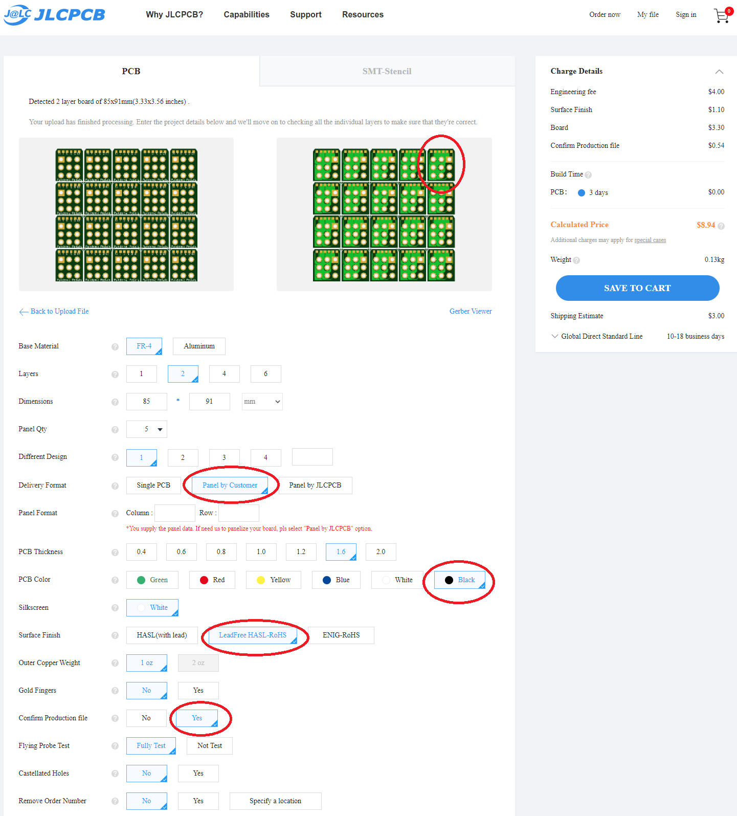
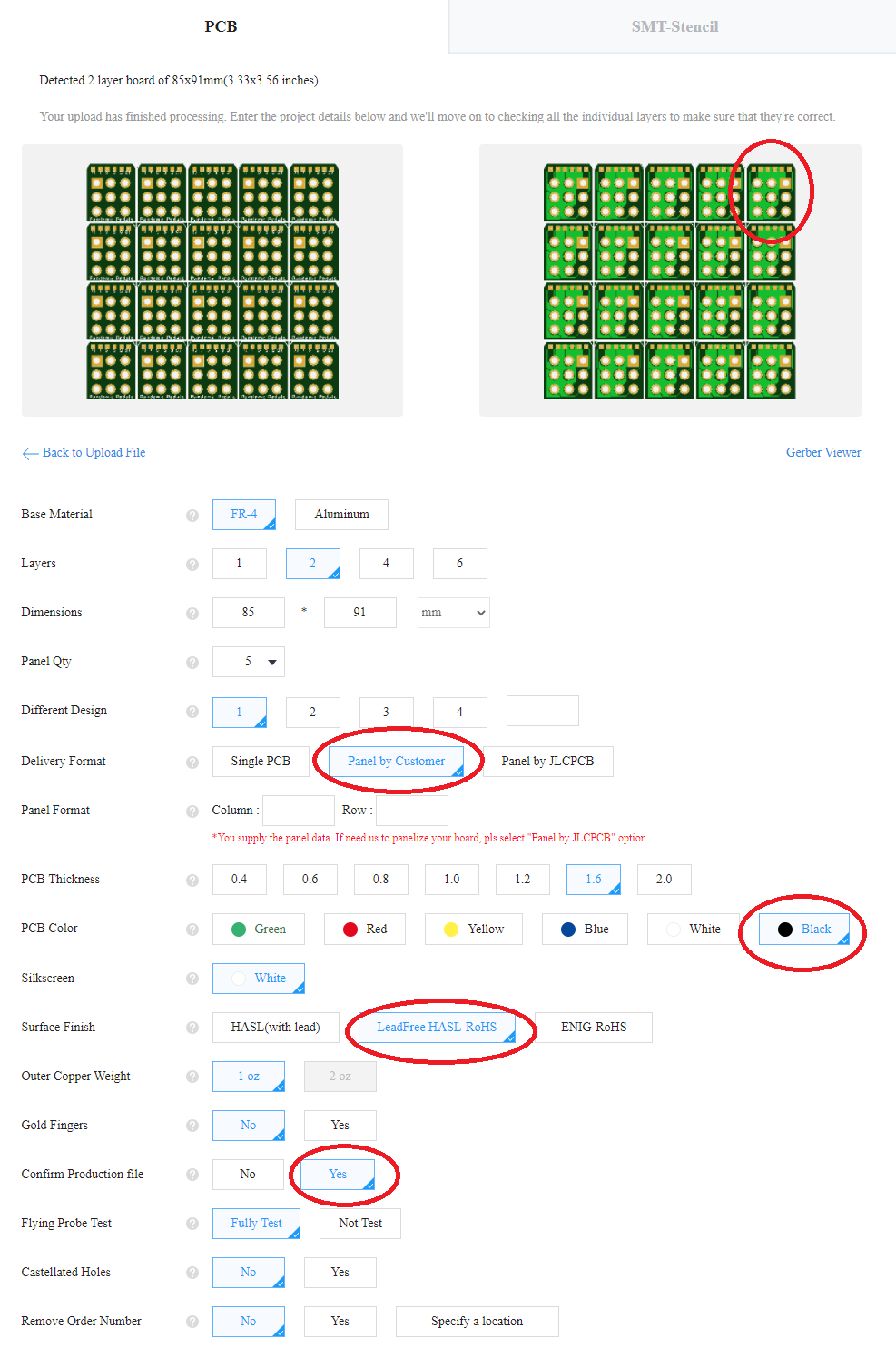
For JLCPCB the settings are:
- must be smaller than 100mm X 100mm [3.937X3.937 inches]
- gaps are 0.4mm X 0.4mm [0.01575 X 0.01575 inches], this leave space for the vcuts
- check ad V-score Lines and Text and Top Stencil
- Hit generate and click through diolog boxes.
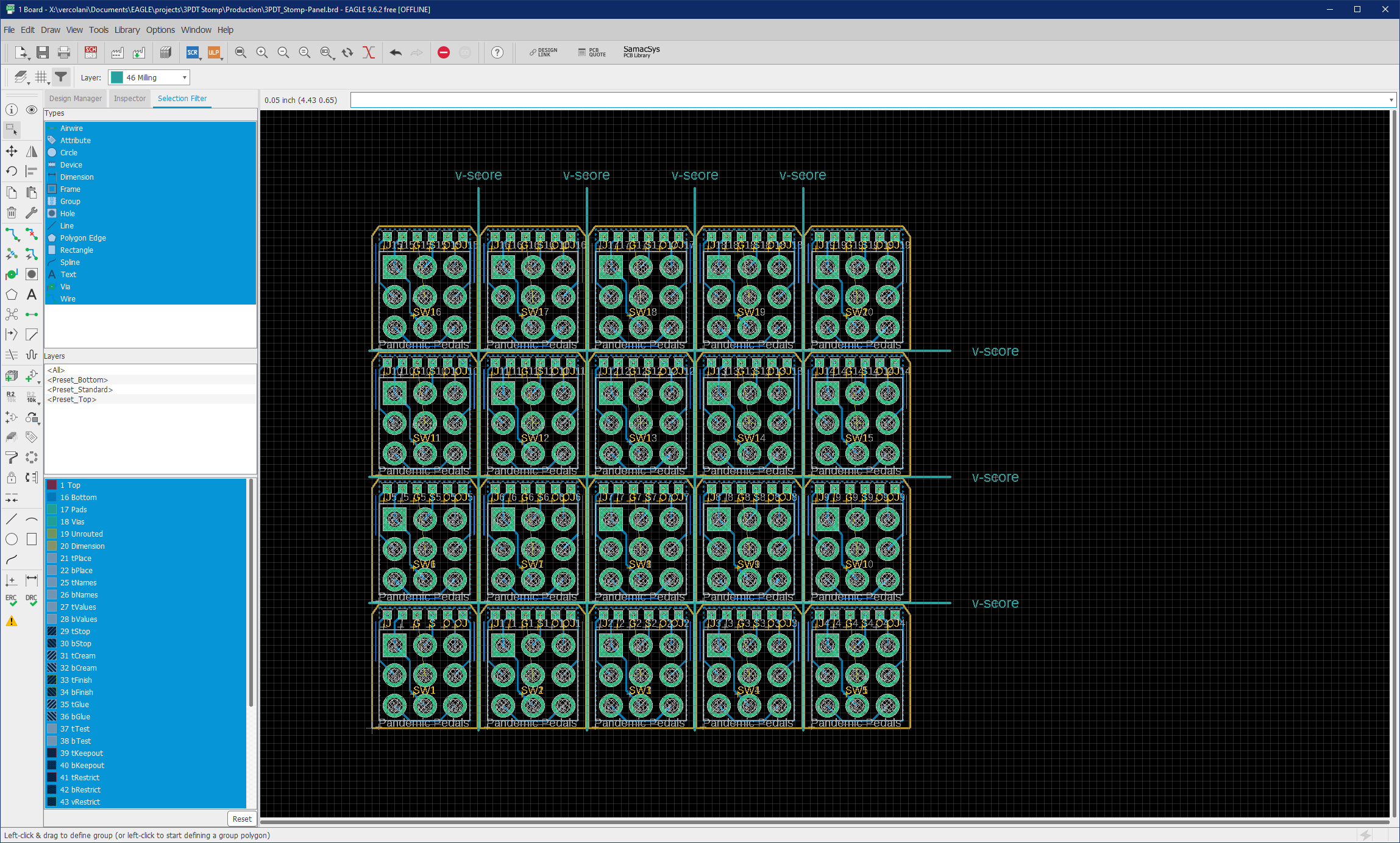
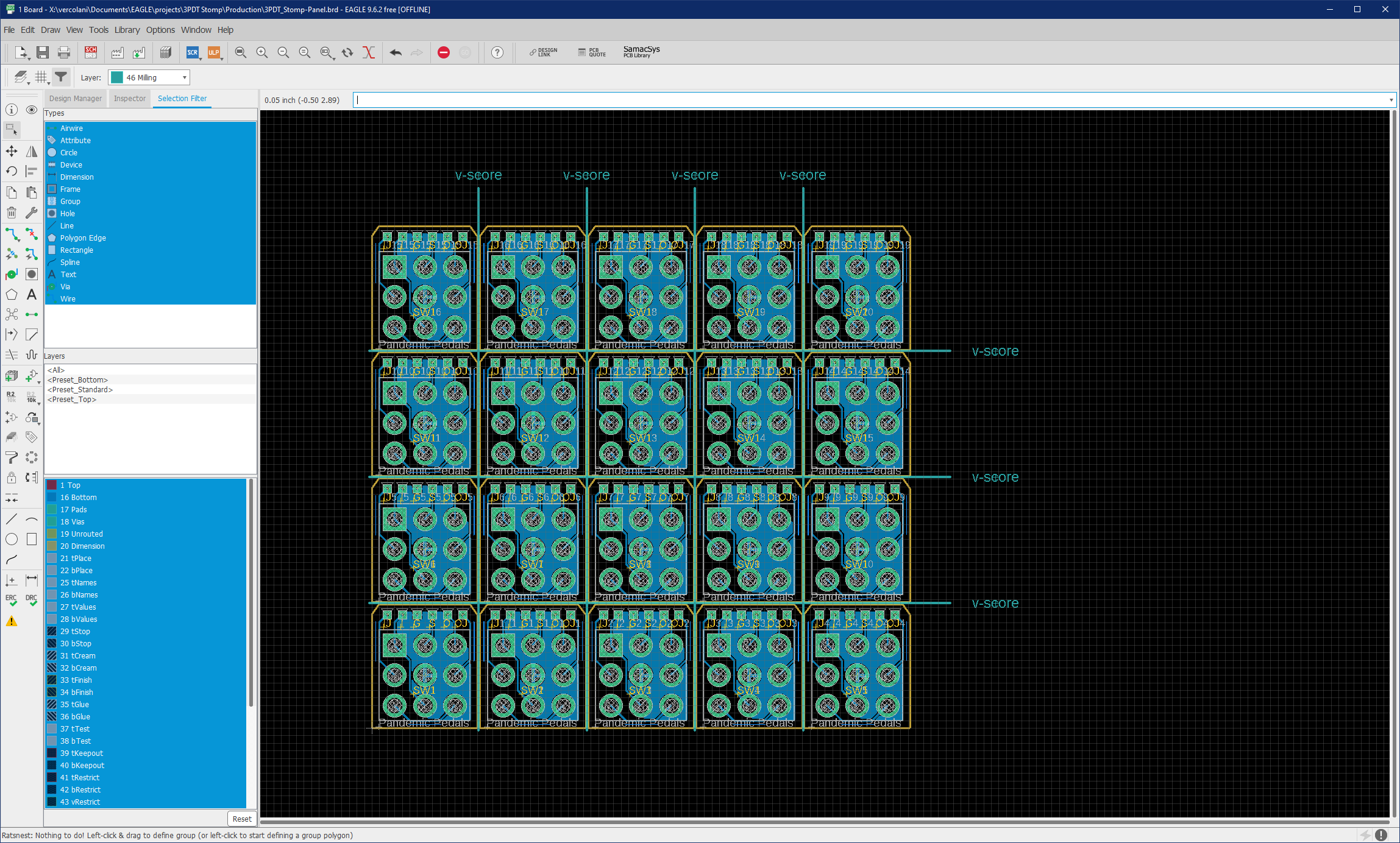
Once the paneling is done you will need to rerun the ratsnest to get your ground plain. This is important or your board will not work correctly. I had this problem with the first one I did.
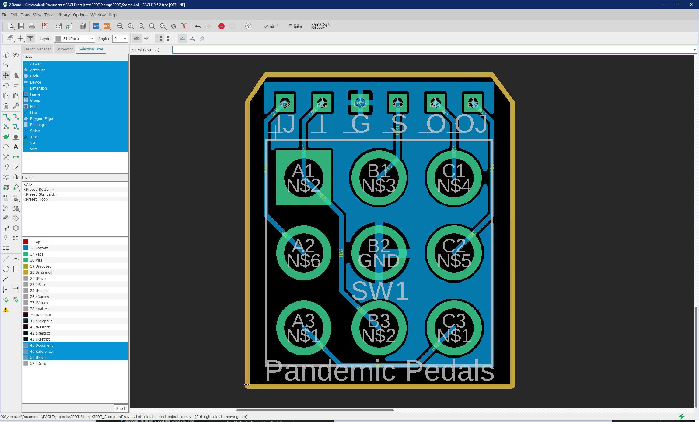
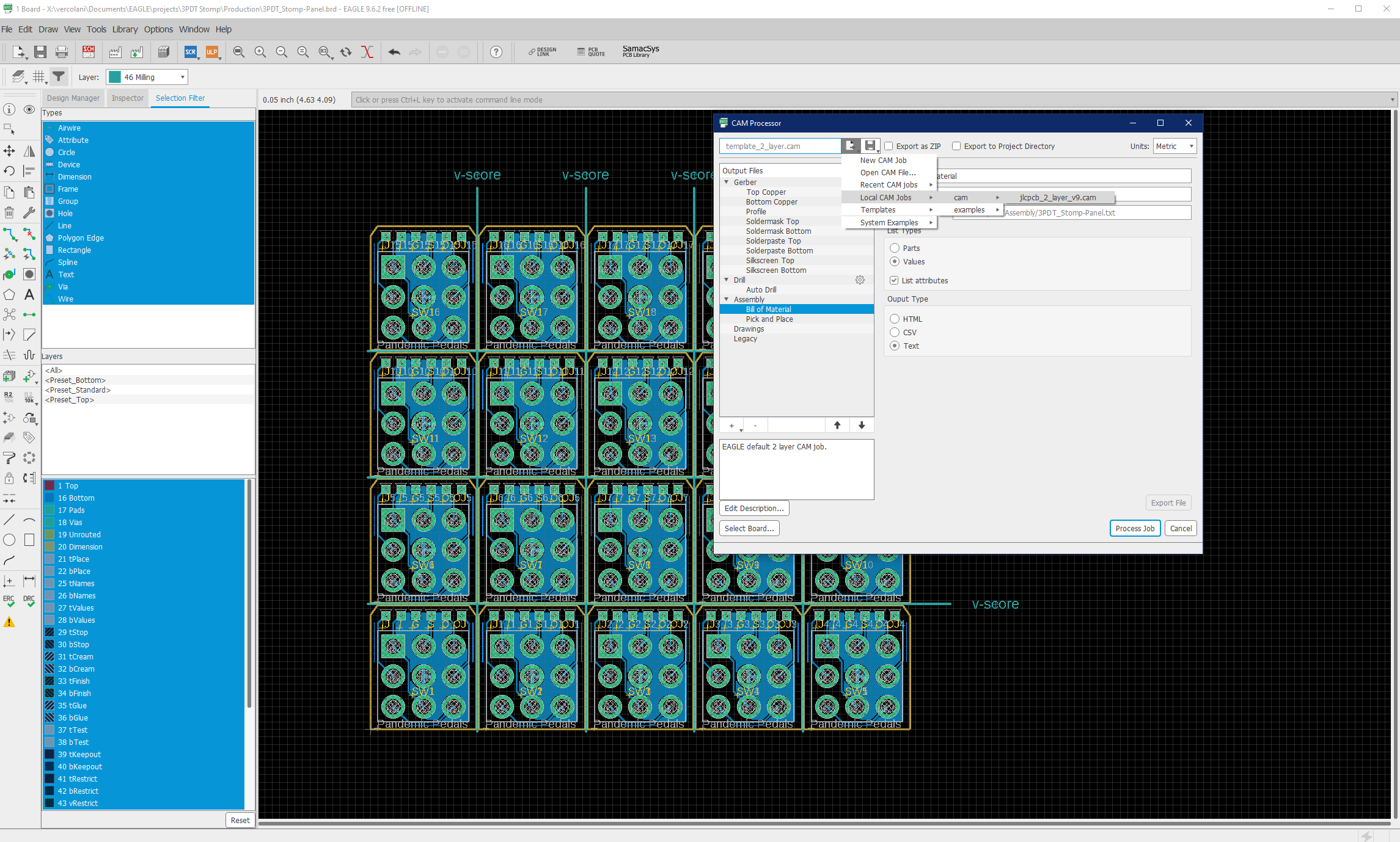
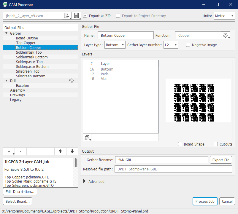
CAM Processor
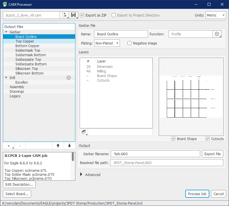
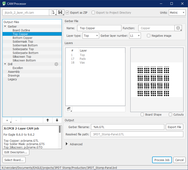
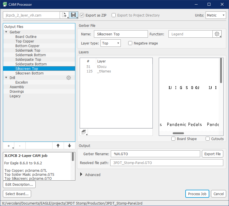
When you open the cam processor you will want to make sure each level has what you want on it.Make sure you add the correct layers to the silkscreen top. I sometimes have to check this several times. Here the panelizer put the correct labels on 125 _tNames and I put the “Pandemic Pedals” on 51 tDocu.
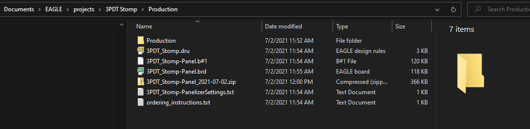
When you are satisfied click on “Process Job” and save the resulting zip file.
This is the directory and all files created in this process.
JLCPCB
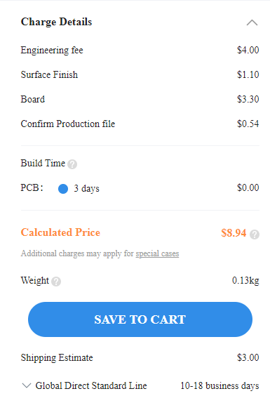
The JLCPCB price for panel by customer for 5, 100mm by 100mm boards is $8 us. This design gets 20 boards per panel. I also make sure that I do the surface finish of LeadFree HASL-RoHS. And I have the confirm the production file. The total with shipping is 12.94 and takes about 2 - 3 weeks to arrive. You can get it much quicker if you want to pay $5 more for the shipping.
For anyone who wants to make this the way it is you can right click and download the zip file here.
These are images of what I have setup and the price.
Note: Make sure that the ground plain and everything looks right in the board image.
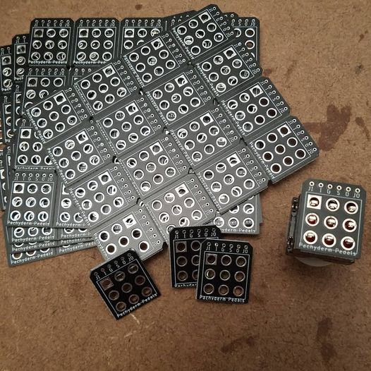
Boards
These are the finished boards from the first batch. I believe the second is better with the name in a better spot and no outline of the stomp.